
fabsolutions
Innovative manufacturing solutions for every challenge. From tiny, to maximum protection, to fully automated.
Reading time: 17 minutes

Individual development solutions that turn ideas into innovations. From the vision to a successful product launch.
Fact: An electronic assembly only works with the right hardware circuit, components and mechanics. The fabsolution service includes the verification of said parts. We check your idea, prepare a feasibility study and a corresponding mandatory booklet. Then let's get to the real work: For the functional testing of electronics, we first develop a prototype.


This and an electronic thermal simulation programme allow us not only to test the electronics extensively, but also to check whether the manufacturing process is working optimally. Finally, we construct the mechanics in which the electronics are embedded. Thanks to detailed 3D studies, we can simulate the perfect fit in advance.
There is only one solution for the best possible functionality: Embedded Systems Engineering – or metaphorically speaking: Hardware and software are identical twins that go hand in hand. With this holistic approach, we ensure from the very start that everything works smoothly during production. This kind of precision requires detailed requirements analysis and exact prototyping — it's done!
Our services in software development cover a variety of areas. We use various microcontrollers – from low power to high performance, from low cost to high tech. At the same time, we also use wired bus systems, interfaces and communication protocols.
The list is long — see for yourself:
In addition, we possess other competencies in the software universe — for example, we develop firmware and program microcontrollers:
And we don't leave computers out of software development either.
Optimally functioning assemblies are based on an optimally planned circuit design — the function is only as good as its form. The challenge here is that the requirements for PCB design have increased significantly in recent years. Electronic components are becoming increasingly complex and smaller, but, conversely, must combine a much greater variety of components. Within fabsolutions, we develop PCB layouts that fully meet these requirements.
And what is more: Due to the PCB unbundling, we are also able to adapt existing circuit designs to certain requirements.
With Mentor Graphics Expedition, we will develop ground-breaking PCB designs or adapt circuits to the prevailing status quo. Without exception, our technologies are state-of-the-art worldwide – regardless of whether they are new developments or optimisations.
During the production of printed circuit boards or a circuit layout, we also take care of other relevant factors: the appropriate dimension of the board, its highest possible degree of miniaturisation, a high packing density, thermal management and ensuring the EMC. At the same time, we design the assembly in 3D so that it can fit into a housing during the layout phase. That special something: The collision check already takes place during layout development.
The basis for the perfect functionality of an electronic assembly is a sophisticated layout, thought out and right down to the nanometer. This also includes the circuit design. Although the requirements in this discipline are becoming ever more complex and demanding, we are able to combine even the most complicated requirements simply and cleverly in a circuit design.
An assembled printed circuit board only becomes a ground-breaking product with the right housing — beautiful shell, smart core. And what is more: A housing protects the interior from a variety of harmful environmental influences. Exactly what other properties, especially mechanical ones, the case still needs, is something we will find out during the development of the PCB layout. On the basis of realistic simulations, we identify which requirements the overall design must meet and which degrees of protection are necessary for this. The protection of the EMC is also integrated into this process. These early collision checks save a lot of time and money in the later implementation.
Four steps to perfect mechanics:
Depending on the field of application of the electronics and the associated challenges of protection class and standard, the technology can also be protected inside the housing — beautiful shell, smart and self-protecting core.
In the development and production of special electronics, two questions regularly pop up: How much does it cost, and how long does it take? The answer is always the same: As little as possible. Even in the early development stage of electronics, we have a firm eye on the costs. During process development, we optimise all production processes, in order to minimise time and costs, while constantly improving quality.
With the best possible solutions for assembly and connection technology and the most suitable selection of suitable components, we can guarantee short, effective and optimised electronics production. And with the right test strategy, we achieve the greatest possible error coverage without losing sight of the effort involved in testing equipment and times.
The development and production of a customer-specific electronic assembly also includes the specific test development. The more complex the device, the more demanding the manufacturing process and testing process becomes.
Test development refers to many test procedures – such as system configuration, programming or parameterisation. And for everything, we have a test.
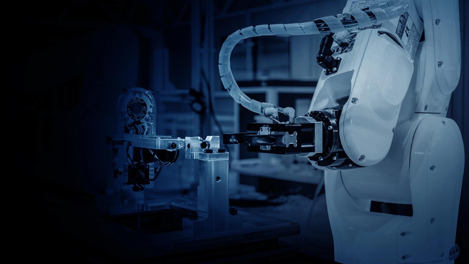
In addition to our own electronics production, we have a fully functional tool shop. This means: We are not only able to produce the solution, but also to produce the means to the end. The main advantage here is that we undercut the time required between development and production many times over. The in-house tool making also brings other advantages with it:
Innovative manufacturing solutions for every challenge. From tiny, to maximum protection, to fully automated.