
fabsolutions
Customer-specific, custom-made production and innovative development solutions.
Reading time: 18 minutes
Innovative manufacturing solutions for every challenge. From tiny, to maximum protection, to fully automated.
CoB technology is an assembly process with comparatively low production costs, but a high miniaturisation potential and considerable complexity in construction. It ensures a good thermal bond to the carrier material. We assemble unhoused semiconductor chips called "dies" in clean rooms of classes 5 and 7 on ceramic or conventional FR printed circuit boards.
We then contact them by wire bonding or by solder or plastic on the printed circuit board. The bonding wires made of gold or aluminium are very delicate and have a diameter that corresponds to only about a third of the human hair. The bonded chips receive a plastic glob top and are thus securely protected.
Chip-on-board offers great flexibility in terms of design, as well as efficient thermal management.
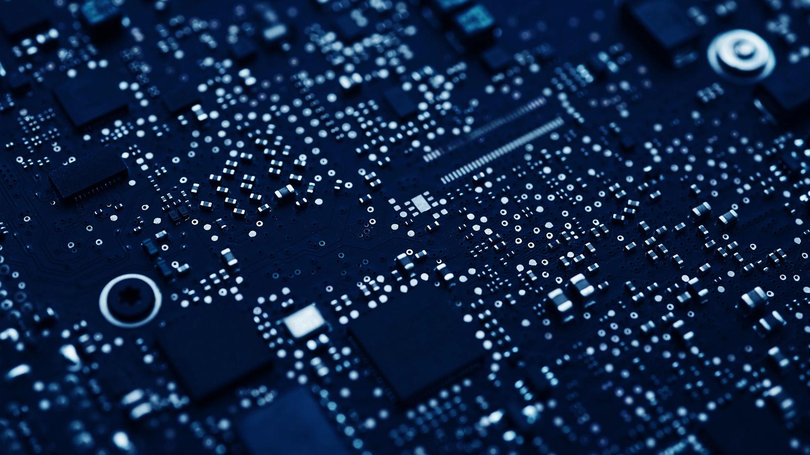
Massive reductions in semiconductor sizes with the improved performance of integrated circuits at the same time – the trend towards miniaturisation continues. The AVT combines microelectronic components with other components, such as PCB, to form an electronic system assembly. Hybrid microsystems and microcomponents — for example, printed circuits, electronics and sensors in a very small installation space — offer a high innovation potential for novel and intelligent products in a wide variety of industries and areas of application.
The increasing variety of applications of sensor and microsystem technology constantly places new demands on the AVT, as well as the packaging of miniaturised assemblies. Thus, a consistently high-quality and cost-efficient adjustment and assembly of the micro-components can only be guaranteed with appropriate automation.
In order to produce customer-specific, highly integrated and miniaturised assemblies, we use the following processes:

The thick-film hybrid technology is an AVT that can be used to produce electronic components and integrated circuits in microelectronics. In fabsolutions electronics production, we use thick-film technology for the production of multilayer PCBs and hybrid circuits. Electronic structures or conductor tracks are screen-printed directly onto ceramic, aluminium or glass substrates. The applied structures are tiny – only 200 micrometres wide, which corresponds to just 0.2 millimetres.
With thick-film hybrid production, we can even realise intersecting conductor paths through the use of insulating layers. The application of the different layers is carried out by repeated printing, drying and sintering for each of the paste systems used in a continuous furnace with a temperature of 850 degrees. Resistors that are also printed on are then trimmed to the desired value with a laser.
After the completion of all printing processes, we compare the generated circuit with the target product and assemble further components by means of SMD or THT assembly with subsequent soldering. We can apply more complex circuits to the substrate by CoB using integrated semiconductors.
The thick-film hybrid technology supports the miniaturisation of electronic assemblies, guarantees good thermal conductivity and enables their use under extreme conditions.
The printing of electronics on glass is a technology that we have offered since 2014, and which has been subject to continuous development since then. Complex circuits can be applied directly to glass using thick-film hybrid technology. Electronic printing on glass not only ensures maximum functionality, it also meets the highest aesthetic requirements.
Electronics printed on glass offer numerous fields of application in lighting, building and medical technology. They can be used as touch panel control units or basic applications, such as LED lights. They are also a welcome addition to the furniture industry — for example, as LED lights placed on glass in glass showcases. Electronics for light sources can be printed directly on a glass pane and thus transform pieces of furniture into interior design home accessories with a contemporary design language.
Direct over-moulding is a special electronic protection process within our fabsolutions manufacturing techniques. After the electronics have been assembled, the printed circuit board is placed in a mould and directly over-moulded with a polymer — hotmelt, thermoplastic, thermoset — in an injection moulding machine. By clever material pairing, even cable sheath or cable conductor can be fused directly to the housing in this work step. The advantage: the assembly and the housing process take place in a matter of seconds, a homogeneous plastic housing sits protectively around the electronics in the form of a monoblock.
We also develop application-specific injection moulds for your electronics.
In medical technology, there are ever more motorised or battery-powered devices. They are used in minimally invasive or robot-assisted surgery, as well as in endoscopy. Many devices must be able to be reused and sterilised for subsequent use. In specific terms, this means that the electronics and sensors used must withstand the special conditions of autoclaving – temperature up to 140 ° C, humid environment and a wash cycle with chemical cleaning agents. In addition, high demands are placed on safety and reliability. The protection should also be economically competitive.
The use of chemically- and thermally-resistant plastics during direct injection moulding makes the protected assemblies washable and sterilisable. The over-moulding has a high thermal stability with respect to autoclaving temperatures between 134 ° C. and 137 ° C. It also has very good hydrolysis stability and good chemical resistance to common, mostly alkaline cleaning agents. Up to 2,500 autoclaving cycles are possible. In addition, the use of biocompatible plastics is also possible.
The most suitable AVT, functioning material management and suitable test procedures – fabsolutions process development ensures that competitive and reliable products are manufactured. The focus is on optimising production times and costs while maintaining the highest quality requirements. In addition, we remain true to our claim of adapting processes exactly to customer requirements and needs.
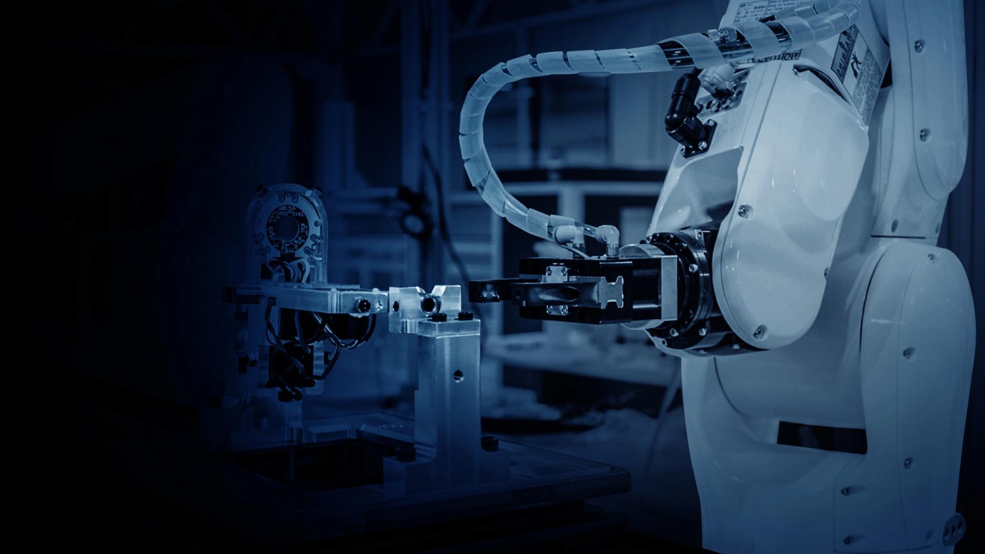
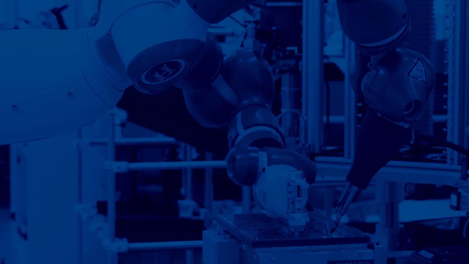
Another equally important aspect is the transfer of the products to series production. We implement these using state-of-the-art technologies, such as robotics, smart camera systems, sensors and much more. In addition, we create automation solutions for large series and manage change orders during the project process. For even more complex requirements, we work closely with an external system integrator who has over 10 years of experience in process development. These include machine design, software development for plant control and robot programming.
When it comes to sample construction and series production, it is important to meet the requirements of each customer exactly. What is said, gets done: This section of fabsolutions is structured and organised in such a way that it ensures low costs, fast delivery times and a fixed series transfer. Now, it is up to the customer to decide on the basis of the above criteria whether the sample production is fully automated, semi-automated or completely manual. At the same time, it is also important to determine in this step whether the design and construction of the prototypes should be done in-house- or should be taken over by us.
In addition to our many years of expertise in sample construction and series production, we also have the special knowledge to select the best possible materials and processes for the goal of "mass production". Without question, the wishes of our customers come first at all times.
In addition to the listed stages, we offer additional tests and measurements. If desired (or even when necessary), we summarise the results and results in a clearly structured report.
Customer-specific, custom-made production and innovative development solutions.