

fabsolutions
Individual development solutions that turn ideas into innovations. From the vision to a successful product launch.
Reading time: 15 minutes
The time-to-market accelerator for your ideas. Prototype construction in 48 hours.
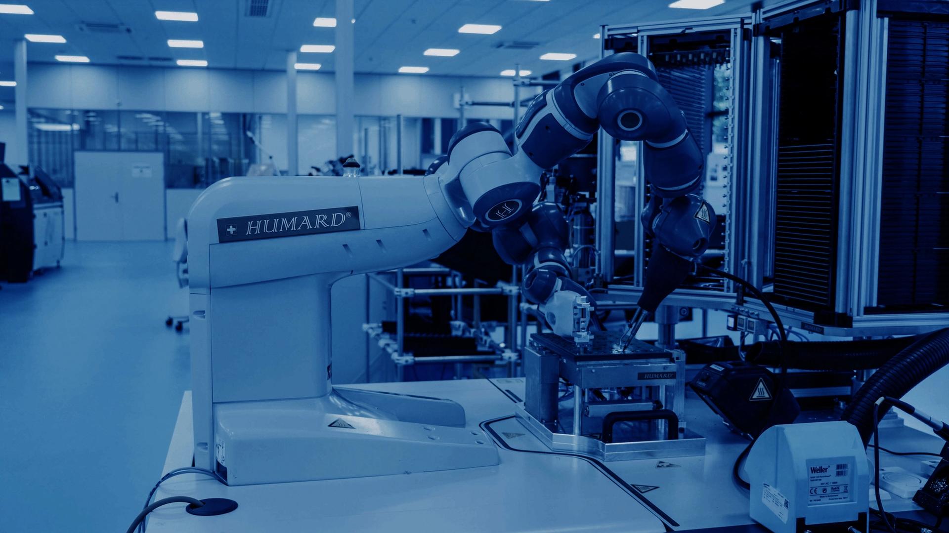
Prototypes play an important role on the way to the mass production of electronic products. They are a first sample of the final product, and are used for the early visualisation and step-by-step optimisation of the electronic assembly. As product cycles become ever shorter, the production of prototypes must also meet increasingly tight deadlines.
fabsolutions Rapid Prototyping will respond to your request with an offer within three days. After three weeks at the latest, you will receive your first assemblies. For the production, we use material provided by you. But we are also happy to take over the material procurement.
The printed circuit boards are equipped by SMD production and THT assembly. Rapid Prototyping of double-layered printed circuit boards can also be carried out directly, we produce a suitable housing using the 3D printing process at the same time. Inspection and testing are carried out by burn-in test, AOI and AXI test as well as FCT. The assembly, commissioning and marking of the assembly, as well as all services are also part of our prototype production.
In CoB technology, unhoused semiconductor chips, also called "dies", are mounted directly on a carrier material. This method is extremely advantageous, since the production costs are comparatively low despite the highly complex structure, whereas the miniaturisation potential is enormous. It couldn't get any better. For sure it can: In LabFab, we put the process under the optimisation magnifying glass. In terms of being innovative, we are taking a big step forward here. Since CoB technologies are used in increasingly complex tasks, it is important to take them to the next level in terms of power, performance and format.
At the LabFab, we are currently conducting intensive research on increasing the temperature resistance of components used, as well as on even thinner wire materials. Especially the latter is not without merit, where assembly processes today are already in the micrometre range. Therefore, it is also important here to rethink innovation.
Researching production technologies that no one has thought of until now – let alone thought possible – is our daily companion. Only with the help of completely new approaches and procedures can electronic solutions be created that outshine everything previously known in terms of both form and function.
Our LabFab, therefore, houses a very special research department: It deals solely with the miniaturisation of electronic components. Revolutionising means looking at things from different perspectives. That's what we do. At LabFab, the mantra is: smaller is better. By focussing on this guiding principle, we are constantly working on reducing the size of our electronic components, but at the same time making them even faster and more powerful. Small, but packs a punch for sure!
In our electronics production, thick-film hybrid technology is used for the production of multilayer printed circuit boards and hybrid circuits under clean room conditions. Conductor tracks are applied directly to ceramic substrates, aluminium substrates or glass substrates by screen printing. We have been continuously improving our know-how in this technology for more than 30 years. In our LabFab, we have the optimal conditions to further research the technology in connection with new substrates. Explicitly, this refers to the screen printing of functional layers on various substrates — such as glass.
Individual development solutions that turn ideas into innovations. From the vision to a successful product launch.